GK Semiconductor's 70/100 mW O-band CWDM4 CW DFB chip (GKCP-1XXX-100M-CW-00, 1271–1331 nm) targets 800G/1.6T optics and external silicon photonics sources. With a ±6.5 nm 25 °C bin, uncooled operation fails over −5 to +85 °C, but works over 25 to 75 °C if binned within 8.5 nm. Section 6 gives the derivation, and the three budgets below outline the math and decision criteria.
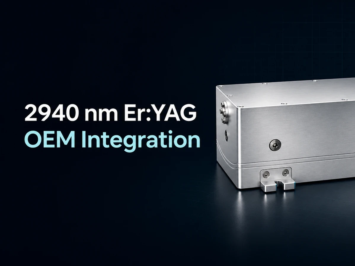
The 2940-200mJ is a modular, lamp-pumped Er:YAG source delivering 200 mJ pulses at up to 10 W average power with an external chiller and delivery optics. System integration is governed by key physical constraints, including a ~1 µm tissue penetration depth, a 50 Hz repetition rate ceiling at full energy, and the requirement for non-silica beam delivery. Furthermore, its high-power emission mandates early mechanical integration of Class 4 safety housing and interlocks.
Where methane's three absorption windows lie | whether 2.3 μm can be used for methane | how much tuning headroom separates the two devices | why 2.33 μm forces a different material system | how sources are configured for simultaneous methane and CO measurement.
BROWSE BY CATEGORY
Latest from GK Semiconductor.
Explore company developments, technology insights and events from GK Semiconductor.
No published stories yet.
This category is ready for verified GK Semiconductor updates.