By Mark Ma, GK Semiconductor|Last updated 10 November 2026
Summary
GK Semiconductor's O-band CWDM4 continuous-wave DFB chip, part number GKCP-1XXX-100M-CW-00, covers 1271 / 1291 / 1311 / 1331 nm at 70 mW or 100 mW per die, with 0.2 nm FWHM spectral width, a 0.09 nm/°C temperature coefficient, sub-90 mA threshold at 75 °C, and 1.4 V operating voltage. It is intended for the parallel single-mode lanes of 800G DR8 / DR4 / 2×FR4 and 1.6T DR8 / 2×FR4, and for use as the external CW source of a silicon photonics modulator.
The answer depends on the operating range and the production wavelength bin. If the datasheet's ±6.5 nm is a 25 °C bin, the die cannot run uncooled from −5 to +85 °C. Over the recommended 25 to 75 °C it can, provided the bin is selected into the 8.5 nm window. Section 6 gives the full derivation; the three budgets below set out the arithmetic and the decision criteria.
Key findings
l A 0.09 nm/°C coefficient consumes 8.1 nm across −5 to +85 °C, or 62% of the 13 nm CWDM4 channel window. What remains for the 25 °C wavelength bin is −3.8 to +1.1 nm: 4.9 nm wide, centred 1.35 nm below nominal.
l The decision hinges on one question: the temperature at which the datasheet's ±6.5 nm is defined. If that figure is a 25 °C bin, uncooled operation across the full range does not hold; if it already covers the range, no tightened selection is required.
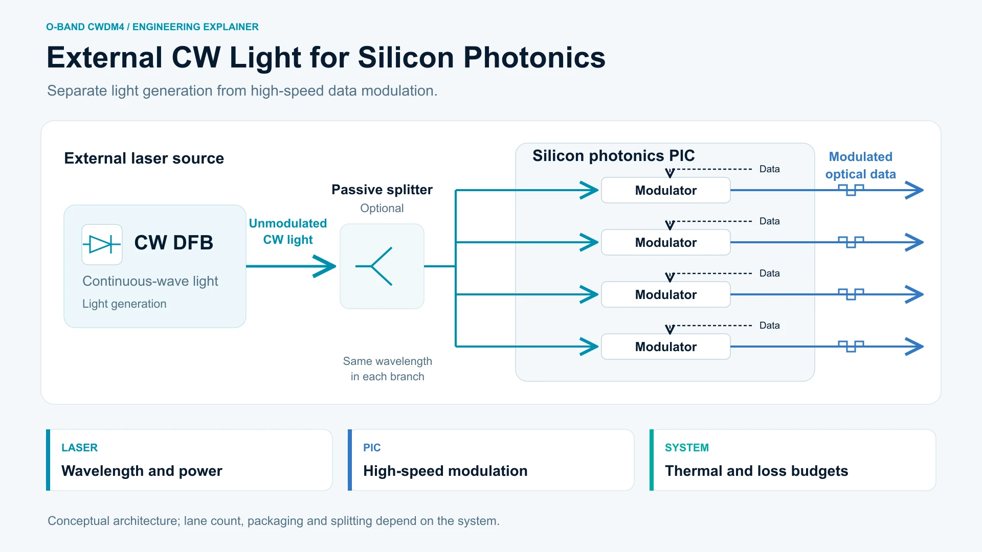
l At 100 mW (20 dBm) with 12 dB link loss, 6.3 mW reaches the modulator in a direct connection and 0.8 mW after a 1×8 split. How many lanes one source serves is set by splitting stages, not by chip power alone.
1. Why does O-band still fit the 1.6T architecture?
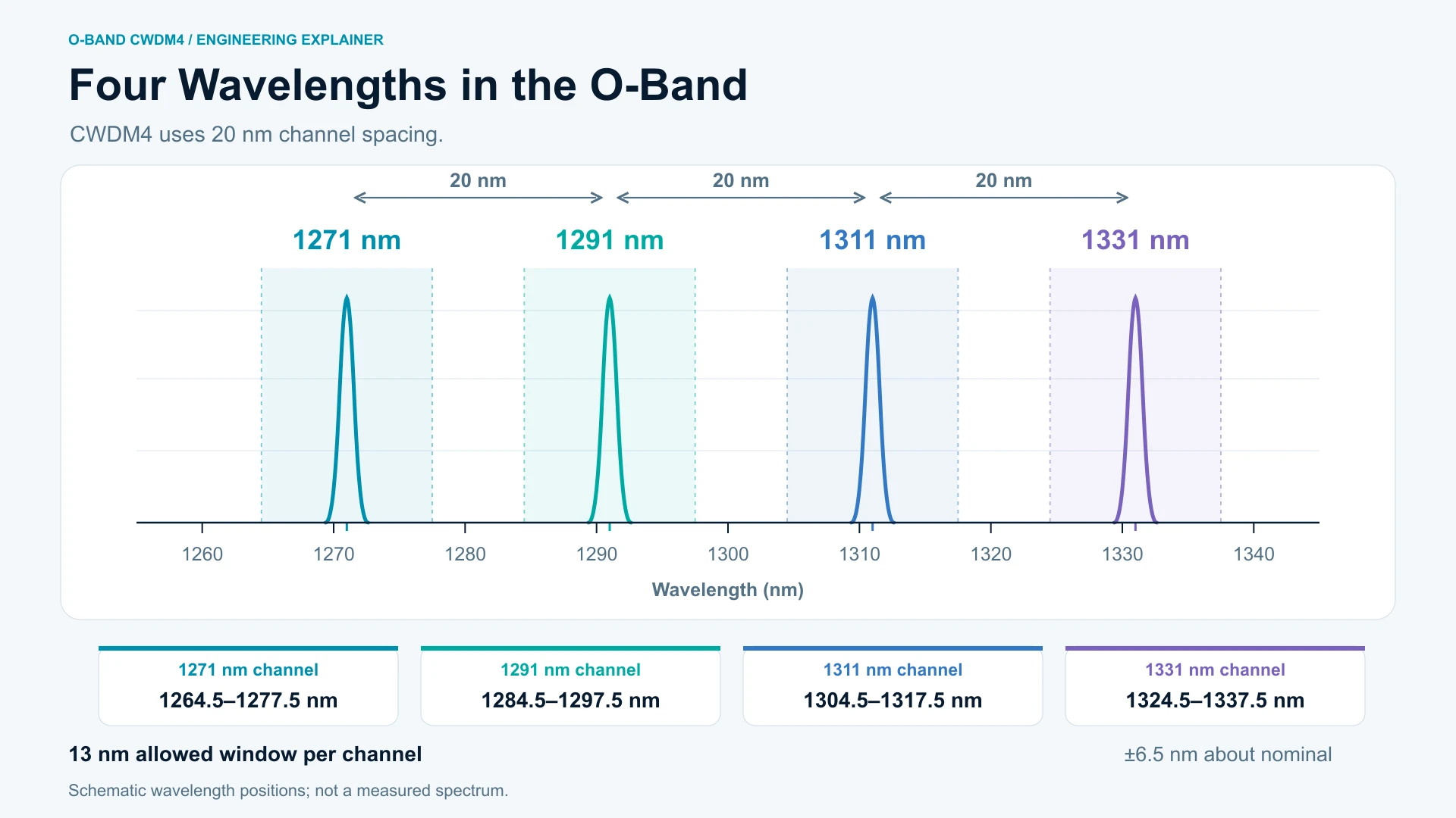
Standard single-mode fiber (ITU-T G.652) reaches its zero-dispersion point near 1310 nm, where material and waveguide dispersion cancel. CWDM4 places four channels between 1271 and 1331 nm, 20 nm apart, all within that low-dispersion region. No dispersion-compensating module is required on the link, and no wavelength locker at the module edge.
The cost is attenuation: roughly 0.35 dB/km at 1310 nm against 0.20 dB/km at 1550 nm on standard G.652 fiber. O-band therefore belongs to the 500 m to 2 km segment: inside the data hall, between buildings, across a campus backbone. Over that distance, dispersion and cost matter more than loss.
What has changed is where the light originates. At 400G and 800G, modulation and light generation began to separate: EMLs for reach-limited lanes, CW DFB driving a silicon photonics modulator on the parallel single-mode lanes. At 1.6T and in co-packaged optics, this separation becomes architectural. The laser leaves the package and moves into a pluggable external laser source (ELS / ELSFP) on the front panel, and the fiber between them carries unmodulated CW light.
OIF published the ELSFP implementation agreement in 2023 (OIF-ELSFP-01.0) and revised it in January 2025 (02.0). The agreement defines form factor, electrical interface and blind-mate connection; it does not address chip specifications. What the chip must deliver is set by the system budget.
2. What three requirements does an external source place on the chip?
| Requirement | Parameter | Evaluation |
| Absolute power per fiber: one source may feed several PIC lanes through a splitter | Output power | Section 7, power budget |
| Threshold behaviour at elevated temperature: the laser runs hotter than the PIC | Threshold at 75 °C | Section 4 |
| Wavelength stability without a local control loop: control electronics no longer sit beside the die | Temperature coefficient | Section 6, wavelength budget |
None of these is a new parameter. Their weight has changed. Deviations that a pluggable module could absorb with a TEC have no compensating element at an external source.
3. GKCP-1XXX-100M-CW-00 specifications
| Parameter | Value | Engineering meaning |
| Lasing wavelength | 1271 / 1291 / 1311 / 1331 ± 6.5 nm | CWDM4 grid, 20 nm spacing (ITU-T G.694.2) |
| Output power | 70 mW / 100 mW | Two bin selections, not one die driven harder |
| Spectral width | 0.2 nm FWHM | ≈ 34.9 GHz at 1311 nm (derived) |
| Temperature coefficient | 0.09 nm/°C | 8.1 nm across −5 to +85 °C (derived) |
| Threshold current | < 90 mA @ 75 °C | Primary input to the TEC decision |
| Operating current | 350 mA | Not split by power bin in the datasheet; confirm per bin |
| Operating voltage | 1.4 V | ≈ 0.49 W electrical at 350 mA (derived) |
| Reverse voltage | < 2 V | Driver and protection limit |
| Duty cycle | 100% | Continuous wave |
| Emitting width | 2.5 μm | Single lateral mode, standard lens coupling |
| Far field, fast / slow | 19° / 16° | Basis for coupling lens selection |
| Cavity / thickness | 1 mm / 100–120 μm | Cleaving and die-attach constraints |
| Recommended temperature | 25 to 75 °C | Normal module thermal envelope |
| Operating temperature | −5 to +85 °C | Uncooled module envelope |
| Storage temperature | −40 to +95 °C | Shipping and warehousing |
| Application fit | 800G DR8/DR4/2×FR4, 1.6T DR8/2×FR4 | Parallel single-mode lanes |
The sibling part 1310-70M-CW (70 mW only, for 400G DR4 / 800G DR4) is specified at 22° fast and 20° slow, against the 19° / 16° of the CWDM4 family. The two do not share a coupling design; lens parameters are set per bin.
4. Why does the 75 °C threshold matter more than the 25 °C figure?
DFB datasheets routinely quote a room-temperature threshold and rarely quote the temperature the design actually operates at. The datasheet for this family gives 75 °C as the upper limit of the recommended range. Threshold current rises approximately exponentially with temperature as carriers escape the active region — a material property, not a process attribute.
Below 90 mA at 75 °C indicates that, at the upper edge of the temperature envelope, the operating point still sits within the driver's linear range. The figure is also the most direct input to the TEC decision: if 100 mW can be sustained at 75 °C, the TEC moves from requirement to option.
A supplier offering only a 25 °C threshold is presenting a data gap, not a specification.
5. What does 0.2 nm mean in CWDM4 and in DWDM?
Convert with Δν = c·Δλ / λ². Across the four channels:
| Channel | 0.2 nm expressed as frequency |
| 1271 nm | 37.1 GHz |
| 1291 nm | 36.0 GHz |
| 1311 nm | 34.9 GHz |
| 1331 nm | 33.9 GHz |
Against a 20 nm CWDM grid, the margin is ample. Note that channels within one module drift in the same direction with temperature, so channel spacing is largely preserved. Linewidth is therefore not the constraint in a CWDM system; the constraint sits at the channel edge, treated in Section 6.
Against a 100 GHz DWDM grid, the constraint is again not linewidth but absolute wavelength. At 1311 nm, 100 GHz corresponds to 0.57 nm, and a 0.09 nm/°C coefficient produces 0.1 nm of shift every 1.1 °C, while DWDM wavelength tolerance is normally specified at the ±0.1 nm level. DWDM requires a TEC — a wavelength-stability problem, unrelated to linewidth. Conflating the two is the most common selection error in this band.
The measurement basis also needs stating. The 0.2 nm figure is normally an envelope read from an optical spectrum analyzer. A FWHM taken with a 0.05 nm resolution OSA is not comparable with a Lorentzian fit from delayed self-heterodyne measurement. The intrinsic linewidth of a CW DFB sits in the MHz range; 0.2 nm is the datasheet's guaranteed limit, not the physical linewidth. Where the intrinsic value matters, request self-heterodyne data separately.
6. Can a CWDM4 chip run without a TEC? Dividing the 13 nm window
Each CWDM4 channel occupies ±6.5 nm, 13 nm in total. For the 1271 nm channel, the permitted range under operating conditions is 1264.5 to 1277.5 nm (CWDM4 MSA). That window must hold two things at once: the wavelength bin established at test, and the drift across the temperature range.
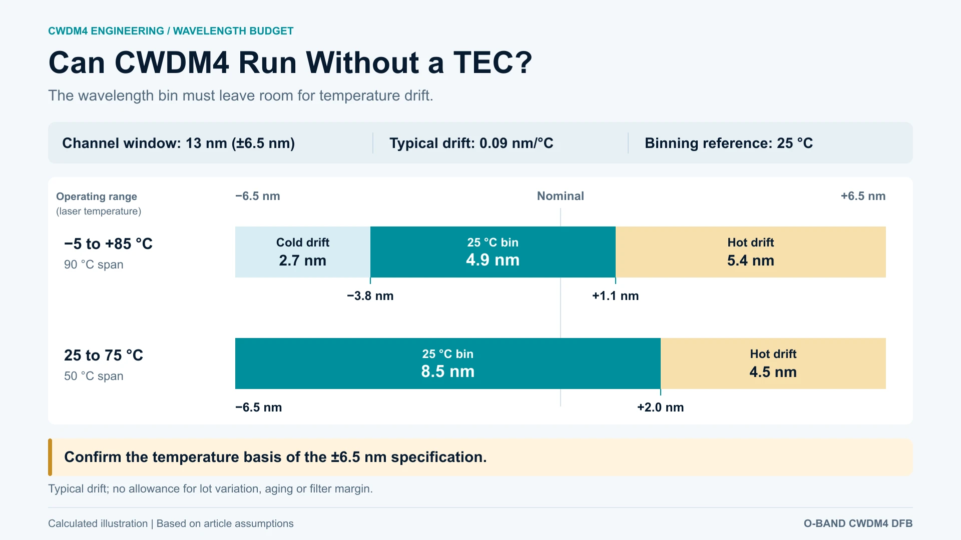
Drift at 0.09 nm/°C, referenced to 25 °C:
| Temperature | Excursion from 25 °C | Wavelength shift |
| −5 °C | −30 °C | −2.7 nm |
| +85 °C | +60 °C | +5.4 nm |
| Full span | 90 °C | 8.1 nm |
Subtracting drift leaves the following window for the production bin:
| Operating range | Drift span | Usable bin window (relative to nominal) | Window width | Window centre |
| −5 to +85 °C | 8.1 nm | −3.8 to +1.1 nm | 4.9 nm | −1.35 nm |
| 25 to 75 °C | 4.5 nm | −6.5 to +2.0 nm | 8.5 nm | −2.25 nm |
The window is not symmetric. Positive drift of 5.4 nm exceeds negative drift of 2.7 nm, so the bin centre must sit about 1.35 nm below nominal. A symmetric ±X nm tolerance will fail: a die selected at +2.4 nm reaches +7.8 nm at 85 °C, 1.3 nm outside the channel window. This is easily lost when a bin width is quoted as ±X nm.
Two decision rules follow:
l If the datasheet's ±6.5 nm is a 25 °C bin, the die cannot run uncooled from −5 to +85 °C — bin plus drift exceeds the 13 nm. Uncooled operation requires the bin to fit inside the 4.9 nm window, or the operating range to be limited to the recommended 25 to 75 °C, where the usable window is 8.5 nm.
l If the ±6.5 nm already covers the full temperature range, the die runs uncooled across that range with no tightened selection.
The two cases lead to opposite conclusions, so the datasheet must state the temperature at which ±6.5 nm is defined and the range it covers. This is the first item to confirm before selecting a part.
Removing the TEC eliminates TEC current, the thermistor loop and control firmware, and reduces the module thermal budget accordingly. The magnitude depends on the module design and is not estimated here.
A TEC remains necessary for any application locked to a specific absorption line, any DWDM grid, any coherent link, and any design that must hold output power within a narrow band over temperature. The last case is often overlooked: DFB slope efficiency also varies with temperature, an effect independent of wavelength.
7. How many lanes can 100 mW drive?
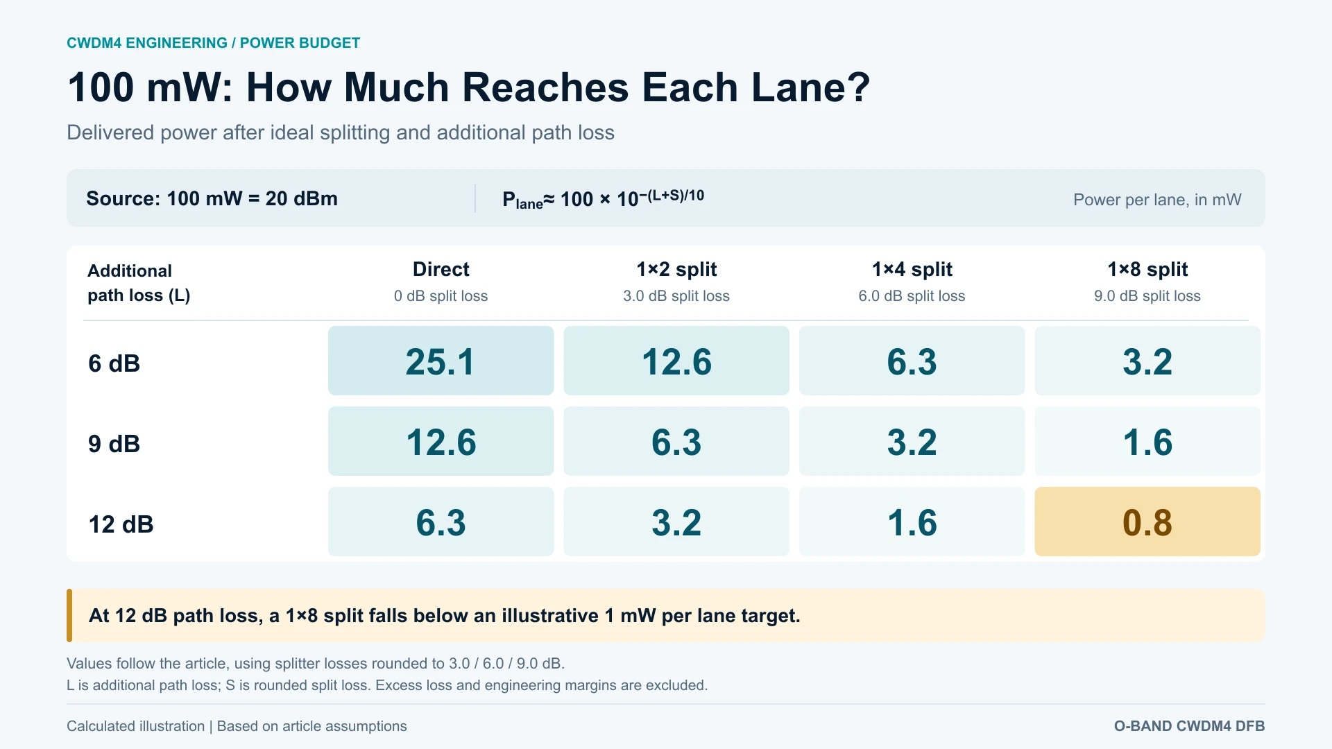
Usable power at the modulator depends on splitter stages and link loss. Theoretical splitter loss follows 10·lg(N): 3.0 dB for 1×2, 6.0 dB for 1×4 and 9.0 dB for 1×8.
100 mW corresponds to 20 dBm. Power reaching the modulator after splitter and link loss (mW, derived):
| Link loss | Direct | 1×2 split | 1×4 split | 1×8 split |
| 6 dB | 25.1 | 12.6 | 6.3 | 3.2 |
| 9 dB | 12.6 | 6.3 | 3.2 | 1.6 |
| 12 dB | 6.3 | 3.2 | 1.6 | 0.8 |
Targeting 1 mW per lane, direct connection and a 1×2 split retain margin at 12 dB link loss, while a 1×8 split leaves 0.8 mW — not enough for eight lanes. A source serving eight lanes should therefore use a higher-power die or fewer splitting stages.
Link loss must be calculated from the actual chip coupling, connectors and routing; no default is assumed here. The table supports order-of-magnitude judgement and does not replace a link budget.
8. How does CW DFB divide work with EML and DML?
A CW DFB does not displace an EML; the two occupy different positions in the architecture.
| Role | Device | Reason |
| Modulated lane, 2 to 10 km, 100G/lane | EML | Integrated modulation, managed chirp, no external modulator loss |
| Modulated lane, very short reach, cost-driven | DML | Lowest cost per lane, adequate to about 500 m |
| External light for a SiPh modulator | CW DFB | Wavelength and power set independently of the modulator |
| External laser source for CPO | CW DFB, higher power per fiber | Source sits off-package; splitter loss must be absorbed |
The main advantage of the CW route is decoupling. The laser can be burned in, screened and binned on its own; the PIC can be tested on its own; and a laser failure does not scrap a complete photonic engine. That advantage is worth more at 1.6T than at 800G, because the value at risk per assembly is larger.
9. What must a specification sheet contain before you request samples?
1. Per-fiber power at the target wavelength, not the family maximum. 70 mW and 100 mW are two bins, not one die driven harder.
2. Threshold and power at the target hot-corner temperature. Request L-I curves at 25, 55, 75 and 85 °C; a 25 °C curve alone is a data gap.
3. The linewidth measurement method — OSA FWHM or self-heterodyne Lorentzian fit, stated explicitly.
4. Wavelength bin and drift distribution: centre, tolerance, measured dλ/dT spread, and the temperature at which the bin is defined.
5. Supply form: bare die, COC/COS or TO package, each implying a different coupling and burn-in flow.
6. End-of-life power margin: accelerated aging at the actual operating current, not only at rated power.
10. Scope and limitations
The calculations above use typical datasheet values and published standards. They support part selection; they do not replace device measurement or link simulation. The following boundaries apply.
l Drift is computed from the typical 0.09 nm/°C coefficient and excludes lot-to-lot spread. Selection should use the measured dλ/dT distribution for the lot rather than the nominal coefficient.
l The bin window assumes wavelength is binned at 25 °C. A different binning temperature, 20 °C or 70 °C for instance, shifts the window without changing its width.
l The power budget counts splitter theoretical loss and link loss only. Connector return loss, polarisation-dependent loss, aging margin and alignment tolerance must be added separately.
l Relative intensity noise, side-mode suppression ratio and polarisation behaviour are outside this article. All three affect bit error rate at high lane rates, but none of them belongs to the three budgets treated here.
l No TEC power, aging life or failure-rate data is given. Those require accelerated aging reports and module thermal simulation.
11. FAQ
Is 100 mW enough to drive a CPO external laser source?
It depends on the number of splitter stages and the link loss; the calculation is in Section 7. Targeting 1 mW per lane, direct connection and a 1×2 split retain margin at 12 dB link loss, while a 1×8 split leaves less than 1 mW and calls for a higher-power die.
Can the TEC be removed?
It depends on how the datasheet's ±6.5 nm is defined. If it is a 25 °C bin, uncooled operation across the full range is not possible; over the recommended 25 to 75 °C the usable window is 8.5 nm, and parts can be selected to it. For DWDM, coherent links, or designs with strict power stability, a TEC is always required, with 0.09 nm/°C as the loop's disturbance input.
What distinguishes 1310-70M-CW from GKCP-1XXX-100M-CW-00?
Same wavelength family, same 0.2 nm spectral width. The first is a 70 mW bin for 400G DR4 / 800G DR4, specified at 22° fast and 20° slow; the second covers four CWDM4 channels at 70 or 100 mW, specified at 19° / 16°. The coupling design is not interchangeable.
Does a 2.5 μm emitting width make fiber coupling easy?
It means the lateral mode matches conventional lens designs well. Fast-axis divergence of 19° still requires collimation, and coupling loss depends on lens choice and alignment tolerance, not on the die alone.
Is the part supplied as die or packaged?
The documented form is the chip-level GKCP part. Package options and a PD-integrated variant are project-level items, not catalogue items.
Is this the same product family as the 1.65 μm and 2.33 μm DFBs?
1310 nm, 1653 nm and 2330 nm are all GK DFB chip part numbers, with wavelength, cavity length and coating set together per project. Material system and capacity allocation are confirmed per part number with engineering.
Are there production 800G module customers that can be named?
No customer part numbers or certification status are disclosed. GK supplies die-level parameters, test data and samples; module-level qualification remains with the customer.
About GK Semiconductor
GK Semiconductor is based in Taiyuan, Shanxi, China and operates IDM capabilities spanning materials, chips, devices, modules and systems. The laser product line covers bands from 780 to 2940 nm, and the DFB chip series includes single-wavelength parts at 1310 nm, 1653 nm and 2330 nm, plus the four-wavelength O-band CWDM4 set.
For an 800G or 1.6T programme, the items worth confirming are the hot-corner operating point, the coupling flow, and the width of the 25 °C wavelength bin — not a single power figure.
l Request the datasheet and test report: L-I-V at multiple temperatures, spectrum, far-field data
l Request engineering samples: 70 mW and 100 mW bins for module-level evaluation
Related: Buried heterostructure vs ridge waveguide lasers · 1653 nm vs 2330 nm DFB for methane TDLAS
Product pages: O-band CWDM4 CW DFB chip · 1310 nm 70 mW CW DFB
Sources and version
l Device parameters: GK product manual, revision 0803, pages P-09 (1310 nm CW DFB) and P-18 (O-band CWDM4). No device data outside the manual is used.
l Standards: ITU-T G.694.2 (CWDM grid), ITU-T G.652 (single-mode fibre), CWDM4 MSA (2014), 100G Lambda MSA, OIF-ELSFP-02.0 (2025), IEEE 802.3df (800G Ethernet).
l Derived values: figures marked "derived" follow the formulas given and can be recomputed item by item; unmarked figures are datasheet values.
l Corrections: any revision to parameters or conclusions takes effect from the update date shown at the top of this page.