Key Takeaways at a Glance
Push the wavelength out to 3–5 μm and silicon and standard InGaAs both drop out; only a handful of narrow-bandgap materials are left on the detection side. MCT has carried the load for decades, InSb is the MWIR classic, and type-II superlattices (T2SL) are the new generation — they hold low dark current at operating temperatures up around 150 K. Every one of these detectors has to be cooled, and a cryocooler is not optional: it is the physical precondition for the technology. For the source side of MWIR (ICL and QCL), see the companion article, Choosing an MWIR Light Source: ICL, QCL, and Antimonide Lasers.
Questions This Article Answers
Which detector materials work in the 3–5 μm band | why high-performance MWIR detectors have to be cooled | how type-II superlattices differ from MCT | where the manufacturing difficulty sits, and which step gates yield.
I. Past 2 μm, the Detector Side Switches Materials Entirely
The boundaries between IR bands are drawn by detector materials, not by wavelength numbers.
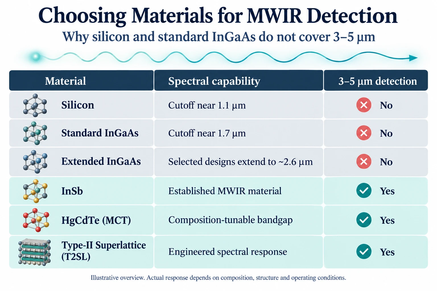
Silicon cuts off near 1 μm, which is what gives 905 nm its cost advantage. InGaAs takes over from 1 μm to 1.7 μm, and extended versions reaching about 2.6 μm are already mature. Go longer, into the 3–5 μm MWIR, and InGaAs stops responding. The narrow-bandgap options left are few.
Four routes carry this band: MCT, InSb, quantum-well infrared photodetectors (QWIP), and type-II superlattices. Barrier designs such as nBn/XBn serve as the reference point for the high-operating-temperature (HOT) direction. Uncooled microbolometers work in the long-wave band, but they measure temperature change rather than counting photons, so they sit in a different performance class and stay out of this comparison.
Switching materials means switching the supply chain, the process equipment, and the vendor list. The 3–5 μm barrier is high, but it sits in that layer, not in the wavelength number itself.
II. Why MWIR Detectors Have to Be Cooled
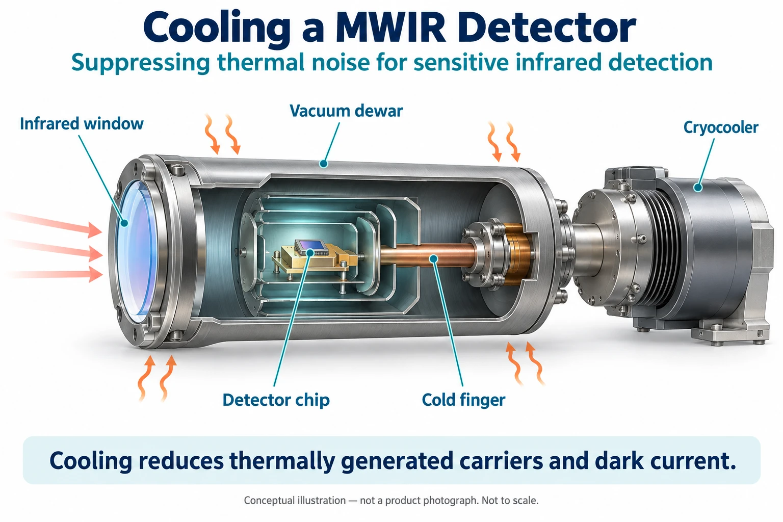
Most high-performance IR detectors are photonic. An IR photon lands on the semiconductor, frees an electron, and the readout turns that into signal. The longer the wavelength, the lower the energy of a single photon, and the narrower the bandgap has to be. Narrow the gap far enough and thermal agitation at room temperature starts pushing electrons across on its own, flooding the device with dark current and thermal noise until the real signal drowns.
Cooling the detector suppresses thermally generated carriers exponentially. The engineering ideal is background-limited performance (BLIP): the detector's own noise drops low enough to ignore, and the system limit is set only by photon fluctuation in the scene background, not by the detector holding itself back. So an MWIR detector ships with a cryocooler. That is not a configuration option; it is the physical precondition.
Different materials need different temperature floors, as the table below shows.
| Material / technology | Band | Typical operating temperature | Characteristics and applications |
| HgCdTe (MCT) | MWIR / LWIR / VLWIR | from ≈ 77 K | Tunable bandgap, widest coverage; the workhorse for decades |
| InSb | MWIR 3–5 μm | 77–80 K | The MWIR classic; high imaging quality |
| QWIP | LWIR / VLWIR | below 40–70 K | Built on mature GaAs processes; vibration-sensitive, common in space payloads |
| Type-II superlattice (T2SL) | MWIR / LWIR | up to ≈ 150 K | New-generation material; holds low dark current at higher temperature |
| Barrier nBn / XBn (InAsSb) | MWIR | ≈ 150 K (HOT) | The HOT reference; sharply reduces the cooling burden |
| Microbolometer (uncooled, for reference) | LWIR | ≈ 300 K | Measures temperature change rather than counting photons; cheap and low-power, but lower performance |
Higher operating temperature eases the size, power, and cost pressure on the cryocooler. T2SL and nBn lift the floor from 77 K to around 150 K, and that is the real reason both draw so much expectation — harder evidence than any performance claim on a datasheet.
III. Type-II Superlattices (T2SL): Where They Differ from MCT
A type-II superlattice (T2SL) is an engineered material system: InAs and GaSb, two lattice-matched materials, grown alternately to atomic-layer precision. Its type-II band alignment separates electrons and holes in space, which yields high quantum efficiency and low dark current.
Response wavelength is set by tuning layer thickness and composition, covering everything from MWIR out to very-long-wave IR. That tunability lets you build to a band instead of being locked to a material's intrinsic bandgap.
Against MCT, type-II superlattices offer clear advantages in material uniformity, large-area manufacturability, mechanical stability, and theoretical performance headroom. They are widely regarded as the leading candidate for third-generation IR detectors, high-performance and multicolor work in particular. MCT's edge is decades of accumulation and the widest band coverage. That gap is real, and admitting it is more useful than overstating our own position.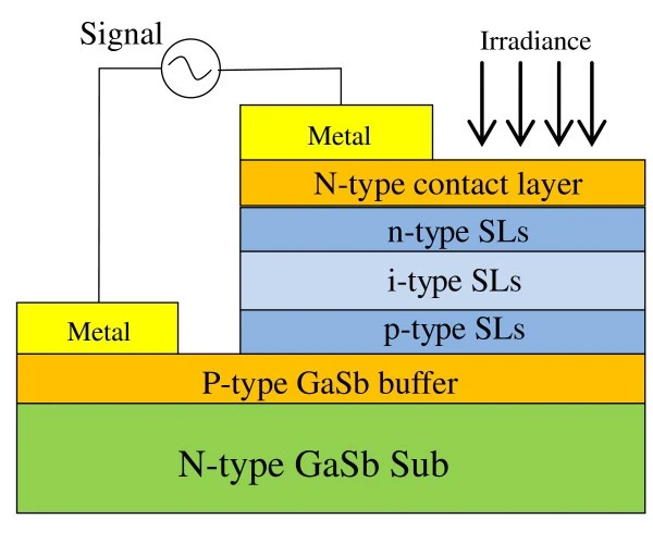
IV. Manufacturing Flow and the Real Yield Barrier
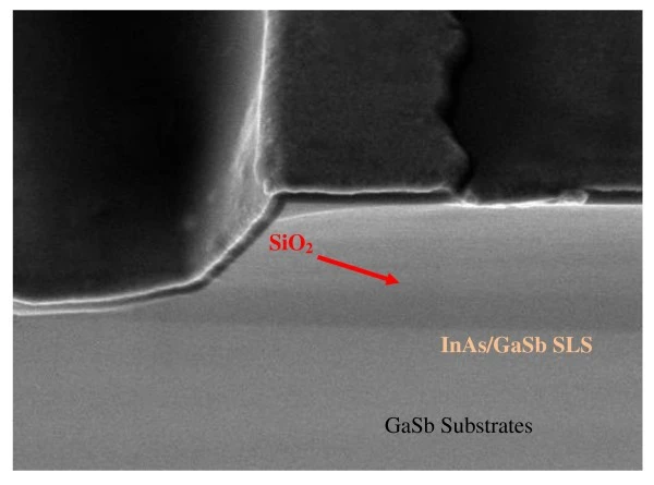
The MWIR detector manufacturing flow runs roughly along one line: MBE growth of the absorber and functional layers → photolithography → dry or wet etching to form pixel mesas → multi-step cleaning → passivation and dielectric deposition (SiO, SiNx) → ohmic-contact metal and indium bumps. From there: flip-chip interconnection → underfill and reinforcement → substrate thinning and backside AR coating → dewar packaging with an integrated cryocooler → electrical and optical test.
Cleaning runs through the entire front end and is where yield is actually controlled. A submicron particle landing on the pixel area can become a short and raise dark current. A single detector array holds hundreds of thousands of pixels, and every failure shows up in the final dead-pixel rate. Get this step wrong and no amount of upstream epitaxy will produce good parts.
The same flow also explains the value of GK's IDM model. We start from wafer epitaxy and carry it through to chips, packaging, modules, and complete systems. Lead times are ours to schedule, with no waiting on upstream suppliers; custom specs can be adjusted at the chip level; and when something goes wrong, we trace it back to a material lot and find the root cause instead of passing it upstream. In long-wavelength IR, where process coupling runs tight, that is the precondition for holding yield and consistency.
V. MWIR Material Systems Side by Side
| Material system | Typical structure | Typical band and products | GK supply status |
| Type-II superlattice (T2SL) | InAs/GaSb, InAs/InAsSb | MWIR / LWIR cooled IR detectors, dual-band focal plane arrays | On the antimonide MWIR/LWIR detector roadmap; models and specs to be confirmed |
| Interband cascade laser (ICL) | InAs/GaSb multiple periods | MWIR gas-sensing lasers, active IR sources | On the roadmap; models and specs to be confirmed |
| Quantum cascade laser (QCL) | InGaAs/AlInAs (InP-based) | MWIR / LWIR high-power QCLs, chemical-detection sources | Not listed in the current product catalog |
| Quantum-well infrared photodetector (QWIP) | GaAs/AlGaAs | LWIR / MWIR QWIP cameras | Not listed in the current product catalog |
| InSb | InSb bulk material | MWIR cooled imaging | Not listed in the current product catalog |
| Barrier nBn / XBn | InAsSb | MWIR high-operating-temperature detectors | Not listed in the current product catalog |
Read the "not listed in the current product catalog" column honestly. What GK ships in volume in the 3–5 μm band is on the source side: antimonide laser chips and bars. On the detector side, models and specs still have to be confirmed project by project.
VI. What to Lock Down Before Requesting a Quote
Target band, MWIR 3–5 μm or LWIR 8–14 μm; the detector's cooling temperature, and who integrates the cryocooler; bare die, packaged part, or a dewar-integrated assembly; and the array size with its dead-pixel acceptance criteria. Until those four are fixed, there is no basis for a quote.
FAQ
Q1 Why can't InGaAs work at 3–5 μm?
InGaAs cuts off near 1.7 μm, and extended products reach about 2.6 μm. Beyond that it stops responding. The MWIR band needs narrow-bandgap materials: MCT, InSb, T2SL.
Q2 Do MWIR detectors always need cooling?
High-performance photonic MWIR detectors do. Uncooled microbolometers can operate in the long-wave band, but they measure temperature change, sit in a different performance class, and are not suited to long-range, high-resolution imaging.
Q3 Where is T2SL stronger than MCT?
Material uniformity, large-area manufacturability, mechanical stability, and holding low dark current at the higher operating temperature of around 150 K. MCT's advantage is decades of accumulation and broader band coverage.
Q4 What is background-limited performance (BLIP)?
The operating state in which the detector's own noise is low enough to ignore and the system limit is set only by photon fluctuation in the scene background. The engineering goal of cooling is to push thermal noise below that level.
Author: Vega (content) Technical review: to be confirmed and filled in by GK Semiconductor's engineering department Updated: 2026-10-14