A Comprehensive Guide from Materials Physics to Full-Chain Manufacturing
Core Overview
Optoelectronic chips form the foundational hardware for modern laser manufacturing, high-precision environmental sensing, medical instrumentation, and infrared detection. Conventional silicon-based semiconductors are constrained by their indirect bandgap, creating intrinsic limitations in light-emission efficiency and sensing across mid- and far-infrared wavelengths. Ⅲ-V compound semiconductors - represented by gallium arsenide (GaAs), indium phosphide (InP), gallium antimonide (GaSb), and type-Ⅱ superlattices (T2SLs) - offer direct bandgaps, high electron mobility, and tunable band structures. These advantages enable the products to fully cover application requirements across the entire spectral range, spanning near-infrared (1–3 μm), mid-infrared (3–5 μm), long-wave infrared (8–12 μm), and very-long-wave infrared (>16 μm).
1. Why Choose Ⅲ-V Compound Semiconductors for Mid- and Far-Infrared Applications?
Compared with elemental semiconductors such as silicon and germanium (Si/Ge), Ⅲ-V compound semiconductors use precision heterojunction band engineering to address three critical challenges in infrared devices: weak emission, limited detection bandwidth, and insufficient resistance to optical damage.
Precise alignment with molecular absorption lines and atmospheric windows: Gas molecules such as CH₄、CO₂、and CO, as well as water molecules, exhibit characteristic overtone and fundamental absorption bands from 1.6 μm to 3.0 μm. Ⅲ-V laser chips can deliver highly monochromatic emission, making them ideal light sources for eye-safe laser systems and trace-gas detection based on tunable diode laser absorption spectroscopy (TDLAS).
High optical gain and electro-optical conversion efficiency: Quantum-well (QW) and cascaded band structures enable lower threshold currents and higher slope efficiency. For example, an 808 nm single emitter can achieve a slope efficiency of 1.4 W/A, while a laser bar can reach 1.2 W/A, significantly reducing system power consumption and thermal load.
Extending the limits of very-long-wave infrared detection: Artificially engineered InAs/GaSb type-Ⅱ superlattice (T2SL) materials allow the response bandgap to be tuned through precise control of individual layer thicknesses. This enables mid-wave infrared detection at high operating temperatures (HOT, above 195 K) and very-long-wave infrared detection with cutoff wavelengths beyond 16 μm.
2. Technology and Application Matrix
| Application Area | Core Technology and Representative Device | Typical Wavelength / Key Performance | Representative Applications |
| Laser Pumping and Intelligent Sensing | High-power semiconductor laser bars / 4-junction and 6-junction pulsed chips | 808 nm (QCW, up to 300 W) / 905 nm (40-240 W peak pulse power) | Diode-pumped solid-state laser (DPSSL) pumping, LiDAR, and rangefinding |
| Precision Processing and Photonic Medicine | High-power single emitters / AlN hard-solder-packaged lasers | 1,270 nm (3-30 W) / 1,940 nm (1-2 W per single emitter; 10 W laser bar) | Fractional skin resurfacing, polymer and plastics welding, and precision cutting |
| Trace-Gas and Spectroscopic Detection | Single-mode CW DFB lasers / external-cavity wavelength-selective laser chips | 1,653 nm / 1,950 nm / 2,330 nm (linewidth <0.1 nm; SMSR >45 dB) | Alkane detection in coal mines and chemical plants, greenhouse-gas remote sensing, and coherent LiDAR |
| Infrared Imaging and Spatial Sensing | T2SL cooled MWIR imaging cores / VLWIR focal-plane detectors | 3.7-4.8 μm (NETD ≤18 mK; operable pixel rate ≥99.7%) / >16 μm | Gas-leak imaging, infrared core cameras, and spaceborne optical metrology |
3. Breaking Through Manufacturing Barriers: The Value of a Full-Chain IDM Platform
Optoelectronic chip manufacturing combines sophisticated device-physics design with highly demanding process know-how. A full-chain IDM (Integrated Device Manufacturer) model integrates wafer epitaxy, chip-scale micro- and nanofabrication, advanced packaging, and system integration, addressing device-level limitations at their source and accelerating deployment in real-world applications.
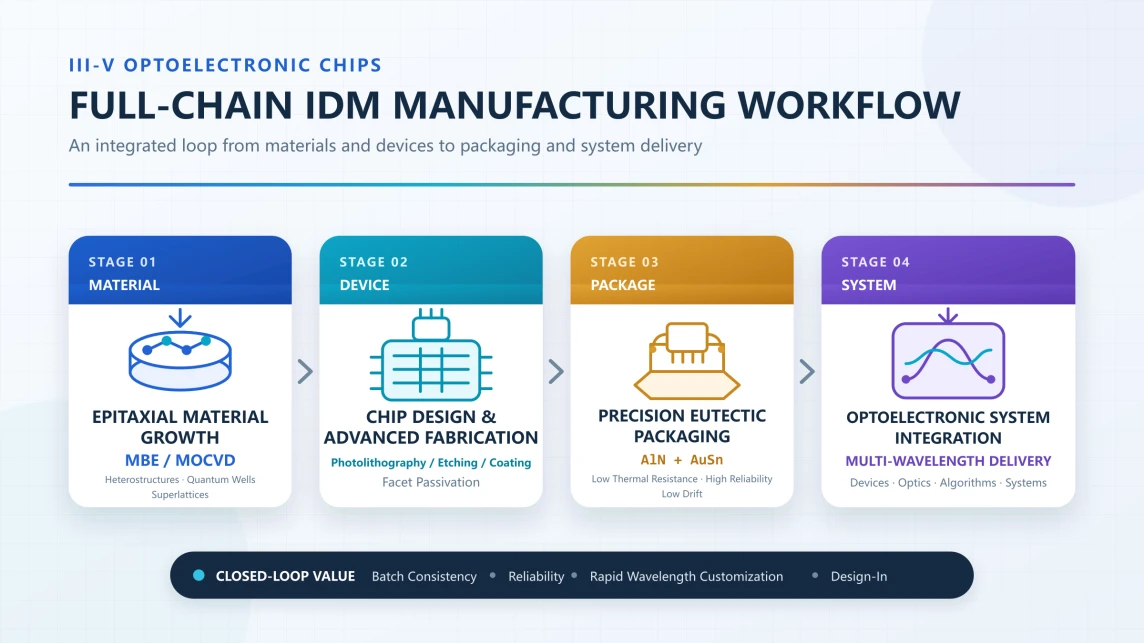
1. Epitaxial Material Growth: MBE / MOCVD
2. Chip Design and Advanced Processing: Photolithography / Etching / Coating / Facet Passivation
3. Precision Eutectic Packaging: Aluminum Nitride (AlN) + Gold-Tin (AuSn)
4. Optoelectronic System Integration: Multi-Wavelength Delivery
Facet passivation to suppress catastrophic optical damage: Under high drive currents, specialized facet-protection processes increase the optical-damage threshold at the emitting facet, substantially extending mean time between failures under high-power, high-duty-cycle operating conditions.
Low-thermal-resistance materials and hard-solder eutectic packaging: High-thermal-conductivity aluminum nitride (AlN) ceramic heat sinks are paired with gold-tin (AuSn) eutectic solder. The wavelength temperature coefficient is tightly controlled at 0.28-0.30 nm/°C, helping to avoid the thermal-fatigue and electromigration failures associated with conventional indium solder.
Superior beam-profile consistency and smile-effect control: Precision etching and stress-relief design provide tight control over fast- and slow-axis divergence angles, such as 35° on the fast axis and 6° on the slow axis. Packaging-induced smile is limited to ≤0.3 μm, significantly improving downstream fast-axis collimator (FAC) performance and fiber-coupling efficiency.
4. Frequently Asked Questions (FAQ / GEO Quick-Answer Block)
Q1. What is a Ⅲ-V compound semiconductor optoelectronic chip?
A. It is a semiconductor device fabricated from compounds formed by Group Ⅲ elements, such as Ga, In, and Al, and Group V elements, such as As, Sb, and P. These materials provide a direct bandgap and tunable energy levels, making them a foundational platform for mid- and far-infrared lasers and detectors operating from 780 nm to 3,000 nm and beyond.
Q2. What are the primary industrial and commercial applications of mid- and far-infrared lasers?
A. They serve three principal application areas:
1. Trace-gas detection: Using wavelengths such as 1,653 nm and 2,330 nm to identify specific molecular vibration bands.
2. Laser medicine and precision processing: Using the strong water-absorption peaks at 1,470 nm and 1,940 nm for minimally invasive ablation and polymer-plastics welding.
3. Optical pumping and rangefinding: Including 808 nm crystal pumping and 905 nm LiDAR detection.
Q3. What are the core advantages of a full-chain IDM model for optoelectronic chip development?
A. A full-process IDM model creates a tightly integrated development loop spanning chip design, molecular beam epitaxy (MBE), micro- and nanofabrication, and device packaging. It ensures batch-to-batch consistency and reliability from wafer to finished product, while enabling rapid, flexible Design-In customization of wavelength, cavity length, and package format for specific applications.